Qualcomm’s datacenter moment isn’t happening on NVIDIA’s timeline.
It’s not for lack of trying—the phone chip giant has been touting its AI accelerators for years, shipping an NPU on every Snapdragon. But the datacenter? That’s where NVIDIA owns the playbook, AMD is catching up, and startups like Cerebras are raising eyebrows. So Qualcomm isn’t chasing the same race.
Instead, it’s pivoting to what everyone in AI infrastructure secretly agrees is the real bottleneck: memory bandwidth.
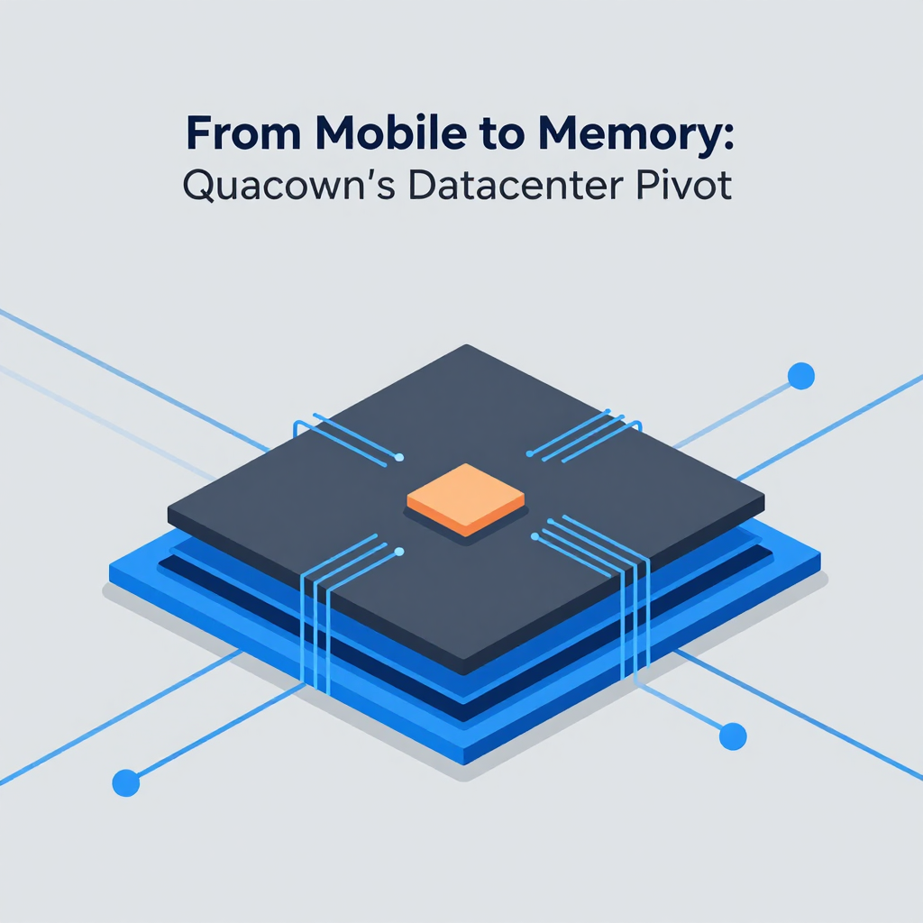
That’s why Qualcomm’s high-bandwidth compute (HBC) architecture—stacking DRAM directly atop XPUs with through-silicon vias (TSVs)—isn’t just clever packaging. It’s a full rethinking of how compute and memory talk to each other.
We’ve all heard the phrase “the memory wall.” It’s the point where adding more compute cores does you no good because your memory can’t keep up. AI inference is especially brutal here: every token-generation loop demands petabytes of data shuffling between DRAM and the compute die, and that’s where power explodes, heat rises, and latency laughs at your优化 dreams.
HBC flips that script. Instead of sending data back and forth across a 2.5D interposer, Qualcomm is burying the compute right under the DRAM stack. Think of it like living and working in the same building: why drive to work when you can just walk up the stairs?
"The value this brings to the industry is lower power consumption, less heat, and that expensive road of silicon interposer that HBM solutions use is no longer needed," Qualcomm’s EVP Tony Pialis explained during the company’s 2026 investor day.
Not that everyone’s buying. Not yet.
Because Qualcomm is using the word "effective bandwidth" like it’s going out of style—and you know what that usually means.
From Mobile to Memory: Qualcomm’s Datacenter Pivot
Let’s be honest: Qualcomm walking into the datacenter market feels like showing up to a heavyweight bout three rounds in. NVIDIA owns this space. AMD is back with MI300-series momentum. And the hyperscalers? They’re either building their own ASICs or locking into NVIDIA’s ecosystem with enough exclusivity clauses to make a monk look hedonistic.
But Tony Pialis didn’t flinch during Investor Day. His answer to the obvious question—are you too late?—was characteristically blunt:
"When the company turns its attention to solve a new problem, we revolutionize the solution and push our way to the forefront."
Fair enough. And if Qualcomm has learned anything from its decades of mobile SoC battles, it’s that execution beats timing. The company has been churning out high-volume chipsets since the 3G days, and that manufacturing muscle translates directly to AI infrastructure—especially when you’re betting on chiplet architectures and fine-feature packaging.
The catch? This isn’t just another CPU effort like the failed Centaur or the canceled Oryon datacenter chips that quietly disappeared into ARM’s acquirement of Marvell’s server division. No—Qualcomm is targeting AI workloads first, specifically inference, and building HBC as the cornerstone of its Dragonfly platform.
And that’s where things get interesting. Because unlike NVIDIA’s HBM-based GPUs, or Cerebras’ monolithic Wafer-Scale Engines, Qualcomm’s approach is born from mobile. The company knows low-power, high-bandwidth memory interfaces inside-out. LPDDR5x isn’t just a spec sheet for Qualcomm—it’s the heartbeat of your phone.
HBC takes that experience and applies it to a 3D-stacked silicon world where DRAM sits directly above the compute die. The upshot? You keep DRAM’s density and capacity while cutting out most of the power-hungry data movement.
In short: more compute per watt, and less need to cool the room.
That’s the story Qualcomm’s telling investors. Now the question is whether the market believes it.
How High-Bandwidth Compute (HBC) Actually Works
Here’s the thing about modern AI chips: they’re mostly moving data, not computing on it.
Take NVIDIA’s latest H200 GPU. You get 4 GB/s of memory bandwidth per pin with HBM3, but that’s only half the story. The rest is latency—the time it takes for a request to travel from the compute die to DRAM and back. In an attention-based LLM, every token-generation step requires fetching the full model weights from memory, and that’s where performance dies.
NVIDIA’s answer? More HBM stacks. The G800 series, for example, uses eight HBM3e stacks to squeeze out 1536 GB/s of bandwidth per GPU. But each stack costs silicon real estate, adds to packaging complexity, and pushes power consumption into triple digits.
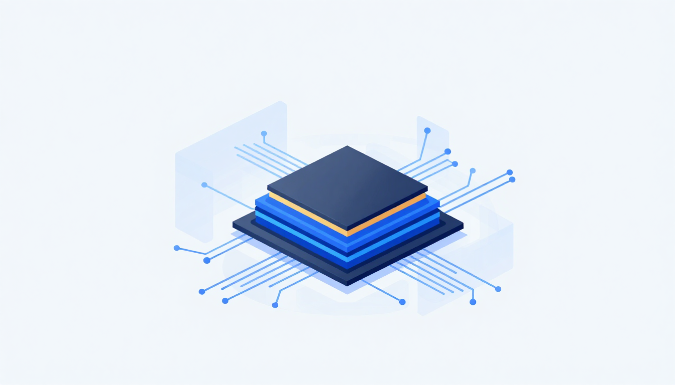
Qualcomm’s HBC takes a different tack: instead of stacking more DRAM above the compute die, it stacks the compute under the DRAM.
The physical layout looks like this:
- Top layer: LPDDR5x DRAM chips (or later-gen High Bandwidth Memory if needed)
- Middle: TSVs—thousands of microscopic through-silicon vias acting as high-speed pipelines
- Bottom: The XPU compute die, optimized for decode-stage inference workloads
That’s it. No fancy 2.5D interposer, no silicon bridges, no multi-million-dollar packaging bills.
The upshot? Data only has to travel a few microns instead of millimeters. That cuts latency dramatically and slashes power because you’re no longer trying to pump data across a highway-sized interconnect.
"Imagine working in the same building that you live in so you only travel up and down," Pialis said. "What does that mean for the highways and the roads that connect the suburbs to the city? Guess what? The roads are clear."
This isn’t just marketing fluff either—PIALIS described performing bandwidth-bound operations like token decoding directly on the base die, where the memory is already attached. In traditional GPU designs, you’d fetch weights from DRAM to a high-bandwidth SRAM cache before processing them. With HBC, you can skip the cache entirely.
The effect is what Qualcomm calls "effective bandwidth"—a measure of how much useful work you can do per second, not just raw gigabytes per second.
For instance, Qualcomm claims its upcoming AI250 will deliver 133 TB/s of effective bandwidth on a single card. Compare that to NVIDIA’s Groq 3 LPUs, which offer just 500 MB of SRAM and 150 TB/s bandwidth in theory—though real-world numbers are usually much lower.
The "18x" bandwidth multiplier Qualcomm mentions between AI200 and AI250? That’s based on effective throughput, not raw interface speed.
Still skeptical?
Here’s the clincher: Qualcomm isn’t claiming record-breaking FLOPS. It’s openly avoiding公布 peak compute figures for AI250, because that’s not the bottleneck. The company wants you to focus on memory bandwidth efficiency instead.
That’s the key differentiation: NVIDIA sells raw performance. AMD tries to match it with ROCm and better pricing. Qualcomm is saying, "Why do you need that much raw performance in the first place? Let’s get more work out of less compute."
It’s a philosophical shift—and one that could pay off if inference, not training, becomes the dominant workload in enterprise AI.
Modular Matters: Breaking Free of CUDA’s Moat
Hardware alone doesn’t win in the datacenter. You need software.
And that’s where Qualcomm’s acquisition of Modular—a startup founded by LLVM and Swift creator Chris Lattner—becomes essential.
Modular’s two big products are Mojo (a low-level programming language and compiler) and Max (an LLM serving stack). The pitch? Write once, run anywhere. Not only does Mojo target GPUs and CPUs, but it also abstracts away the quirks of NVIDIA’s CUDA, AMD’s HIP, and other vendor-specific runtimes.
For Qualcomm, this is the missing piece. The company can build a killer AI accelerator, but without tooling and frameworks, no one will touch it. AMD spent years battling this fate—its hardware was competitive, but ROCm’s instability kept customers locked into NVIDIA.
Modular changes that equation. Developers can now write highly optimized AI applications knowing they’ll run on Qualcomm, NVIDIA, or AMD hardware without needing to maintain three separate codebases.
And that’s not just for model training. Max, Modular’s serving platform, is designed from day one to run heterogeneous deployments—so you could use NVIDIA GPUs for prompt prefill and Qualcomm AI250 chips for decode, all under one unified runtime.
"The big idea is that users should be able to write highly performant AI apps that’ll run regardless of the underlying hardware," Lattner told me in an email exchange last week.
It’s a subtle but powerful shift: instead of forcing customers into one ecosystem, Qualcomm is building an ecosystem that welcomes everyone.
NVIDIA may not love it. But hyperscalers? They’ll kiss your ring for this.
Dragonfly’s Roadmap: From AI200 to AI300
Qualcomm isn’t talking about a single chip. It’s talking about an entire AI infrastructure platform called Dragonfly.
Here’s what we know so far:
-
AI200-series racks ship in 2026. These use the existing Oryon-based architecture, sans HBC, and serve as a stepping stone to the real payoff.
-
AI250, the first HBC-powered system, launches in 2027. According to Qualcomm’s investor deck, it will offer:
- Up to 133 TB/s of effective memory bandwidth
- 768 GB of memory per card (Massive LPDDR5x or HBM3e options)
- Nopeak FLOPS disclosure—but heavy focus on decode-optimized performance
-
AI300, the second-gen HBC platform, drops in 2028. That’s where Qualcomm promises a 54x bandwidth boost over AI200—though what that means in real-world benchmarks remains to be seen.
The company also confirmed it’s working with Microsoft and Meta on multi-year deployments of HBC-based accelerators, though neither has publicly named AI250 or Dragonfly in official announcements. Meta even sent Mark Zuckerberg to Investor Day, a rare sign of commitment for an unproven hardware vendor.
In reality, the AI250 won’t replace NVIDIA GPUs. Instead, Qualcomm is targeting disaggregated inference architectures where HBC accelerators handle memory-bound decode steps while GPUs or CPUs manage prompt processing. That’s a smart wedge—few customers want to rip and replace their entire AI stack at once.
Qualcomm is betting that memory bandwidth efficiency, not raw compute power, will be the next battleground—and that hyperscalers are desperate for alternatives to NVIDIA’s pricing and exclusivity.
Time will tell if HBC can break the memory wall. But it’s absolutely worth watching.
The Bottom Line: Why This Changes the Game
Qualcomm’s datacenter play isn’t about matching NVIDIA chip-for-chip. It’s about redefining what “performance” means in AI infrastructure.
Where NVIDIA sells you a Ferrari, Qualcomm is offering a hybrid electric coupe that gets 300% more miles per gallon—same top speed, half the fuel bill.
The combination of:
- 3D-stacked HBC architecture (compute under memory)
- LPDDR5x or HBM5 interfaces
- Software abstraction through Mojo/Max
- Already-backed deployments with Microsoft and Meta
…creates a credible alternative to the current duopoly.
Yes, Qualcomm is late. But if you’re building a next-gen AI cluster today and can’t afford to be locked into one supplier, your options are limited.
NVIDIA’s strength is its ecosystem. AMD’s is pricing. Intel’s? Well, Intel’s is trying.
Qualcomm’s play? It’s offering what the hyperscalers want most right now: choice, efficiency, and an escape hatch from vendor lock-in.
And if HBC actually delivers even half of its promised bandwidth-per-watt, that choice could become a must-have.
The memory wall isn’t just an engineering problem. It’s the single biggest economic constraint on AI at scale.
Qualcomm isn’t just trying to climb over it.
It’s trying to bury the wall—and build a taller building on top.