The 2028 Silicon Horizon
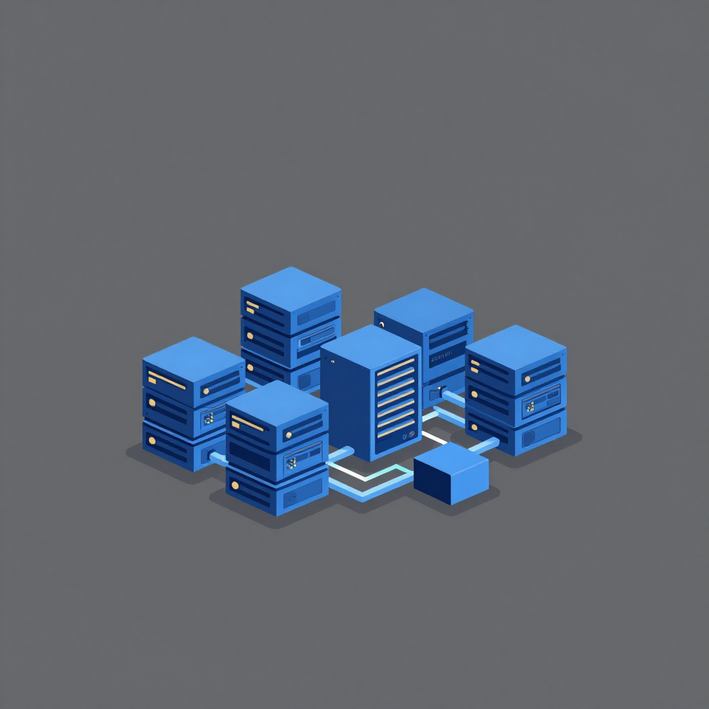
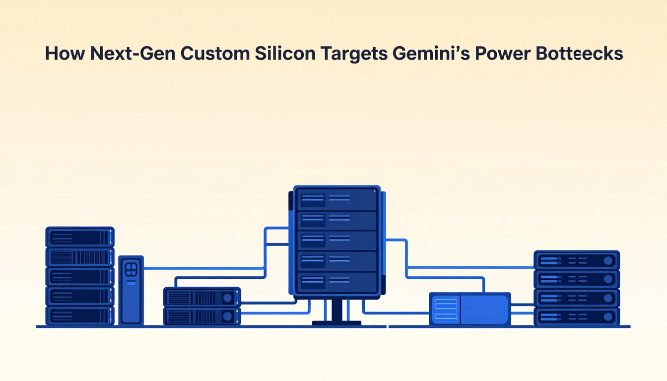
Alphabet isn't waiting around for standard hardware roadmaps to solve its inference costs. The company is actively designing a new in-house server chip codenamed "Frozen v2," tailored specifically to run its flagship Gemini AI models. First reported by The Information and targeting a 2028 deployment window, the silicon project aims for a massive architectural efficiency leap: generating six to ten times more tokens per unit of power than Google's current AI hardware lineup.
When asked about the project, Google declined to confirm specific details but offered a clear statement on its engineering philosophy: "Our teams are constantly researching and experimenting with new innovations to deliver maximum performance and efficiency for our users and customers," the company told TechCrunch. "While not every project moves into production, this rigorous exploration is central to our full stack approach. By co-designing our hardware and software from the ground up, we ensure our systems are integrated and highly optimized for real-world workloads."
That full-stack philosophy is no longer just an abstract engineering goal. It is an economic requirement. As context windows expand into millions of tokens and autonomous agent workflows require persistent model loops, inference energy efficiency is becoming the primary operational wall for cloud hyperscalers.
The Efficiency Math Behind Token Delivery
Evaluating chip performance strictly by floating-point operations per second (FLOPS) is a relic of classical high-performance computing. In modern generative AI infrastructure, the real throughput bottleneck is energy efficiency measured in tokens generated per watt. If Frozen v2 hits its target of 6x to 10x token efficiency over current Google silicon, the downstream operational impact will be profound.
Generative workloads—especially multi-step reasoning agents—spend considerable energy idling while waiting for memory access during token generation. Standard graphics processing units push raw compute density, but they burn substantial power maintaining high memory bandwidth across broad target workloads. A domain-specific processor optimized explicitly for Gemini’s architecture allows Google engineers to cut unnecessary logic paths, optimize on-chip memory caches, and tailor data pipeline timing for exact model execution dynamics.
Consider what a 6x efficiency multiplier means inside a multi-gigawatt data center footprint. Power consumption directly limits total rack density in modern facilities. When power envelopes constrain how many chips can run in a single row, doubling energy efficiency effectively doubles available compute output without building new electrical substations. For enterprise teams running long-running agentic workloads, higher efficiency per watt translates directly into lower cost per million tokens and lower operational latency (see our context on 2026 AI Datacenter Infrastructure).
Wall Street, CapEx, and the $190 Billion Equation
The timing of the Frozen v2 leak reflects the broader pressure mounting across public tech companies. Alphabet has signaled planned capital expenditures between $180 billion and $190 billion this year alone, a staggering commitment driven almost entirely by AI infrastructure buildouts.
For quarters, Wall Street investors have voiced anxiety over these massive capital commitments. High spending is tolerable during early technology shifts, but investors eventually demand proof of sustainable returns on investment. Buying off-the-shelf accelerators from external suppliers eats directly into cloud profit margins. Building custom silicon captures that hardware margin internally, reducing long-term capital expenditure per deployed compute node.
Financial markets responded immediately to the news. Following the disclosure of the Frozen v2 project, Alphabet's stock rose approximately 3% on Monday morning ahead of its weekly earnings report. Investors recognized that long-term margins in the AI era won't be won by purchasing third-party hardware at premium prices; they will be won by companies that own their silicon supply chain from transistor to API endpoint.
Breaking Free from the Third-Party Silicon Trap
Alphabet's push with Frozen v2 is part of a structural shift across the technology industry: major AI labs are aggressively working to break their dependence on third-party suppliers, most notably Nvidia. While Nvidia's general-purpose GPUs remain the default choice for initial model training, relying exclusively on a single hardware vendor leaves tech giants vulnerable to supply chain bottlenecks, allocation limits, and tight gross margins.
Google was an early pioneer in this space with its Tensor Processing Unit (TPU) architecture, but its competitors are rapidly catching up with their own custom hardware initiatives:
- OpenAI announced its first custom inference processor, codenamed Jalapeño, to optimize its model serving pipelines (see our analysis on OpenAI's Jalapeño Chip).
- Anthropic has entered discussions with Samsung to establish custom chip manufacturing partnerships aimed at securing dedicated silicon capacity.
- Meta continues to scale production of its internal MTIA accelerators (detailed in our report on Meta's MTIA Chip Strategy) to offload internal recommendation and model inference workloads.
This ecosystem-wide pivot isn't about eliminating third-party GPUs entirely. It is about strategic leverage. By maintaining production-ready internal chip designs like Frozen v2, hyperscalers gain hardware flexibility, secure capacity during industry-wide chip shortages, and keep external suppliers honest during procurement negotiations.
Co-Designing Hardware for Next-Generation Agents
The shift toward custom processors like Frozen v2 signals an important evolution in how AI systems are built. In early AI development, software models were constrained to run on whatever hardware was available off the shelf. Today, hardware is built around the exact mathematical structure of the software models it serves.
Google's emphasis on co-designing hardware and software from the ground up gives it a unique advantage in agentic infrastructure. Agentic workflows require continuous model calls, tool interactions, and dynamic context retrieval. When the chip architecture, model weights, and compiler stack are engineered by the same teams under one roof, micro-optimizations accumulate across the entire operational stack:
- Memory Subsystem Alignment: Caching intermediate token states directly in high-speed, on-chip memory reduces off-chip memory traffic during deep multi-step reasoning.
- Compiler-Level Scheduling: Custom compilers can map Gemini-specific tensor operations directly onto dedicated hardware execution units without generic abstraction overhead.
- Thermal and Power Budgeting: Dynamic voltage and frequency scaling can be tuned specifically for token generation bursts, lowering data center thermal loads.
Targeting a 2028 release window means Frozen v2 is being designed for model architectures that don't even exist yet. It assumes that future Gemini models will require massive parallel execution with strict energy caps. Whether or not Frozen v2 reaches mass production in its current form, Alphabet's investments in custom silicon guarantee that the battle for AI dominance will be fought as much in the semiconductor fabs as in the algorithmic research labs.